- 您现在的位置:买卖IC网 > Sheet目录475 > MC13852-900EVK (Freescale Semiconductor)IC MC13852 EVB 900MHZ
�� �
�
�Applications� Information�
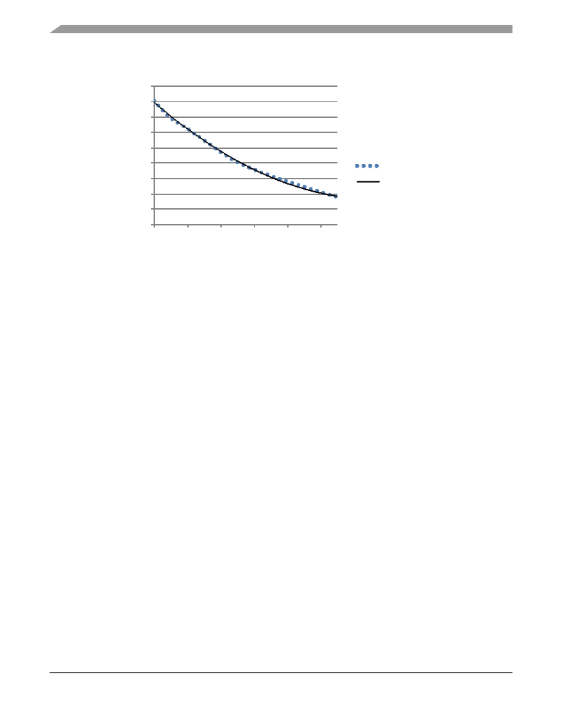
�Figure� 6� shows� the� Icc� current� drain� for� a� range� of� values� for� the� external� bias� resistor� Rbias.�
�6.5�
�6�
�5.5�
�5�
�4.5�
�4�
�3.5�
�3�
�2.5�
�2�
�y� ?� =� ?� 1.7619x� 2� ‐� 8.5883x� ?� +� ?� 13.293�
�R2� ?� =� ?� 0.9983�
�Icc� ?� mA�
�Poly.� ?� (Icc� ?� mA)�
�1.1�
�1.3�
�1.5�
�1.7�
�1.9�
�2.1�
�Rbias� ?� value� ?� (kohm)�
�Figure� 6.� Icc� vs.� Bias� Resistor� R1� Value�
�3�
�Applications� Information�
�The� MC13852� LNA� is� designed� for� applications� in� the� 400� MHz� to� 1� GHz� range.� It� has� three� different�
�modes:� High� Gain,� Low� Gain� (bypass)� and� Standby.� The� LNA� is� programmable� through� the� Gain� and�
�Enable� pins.� The� logic� truth� table� is� given� in� Table� 3� .� The� internal� bypass� switch� is� designed� for� broadband�
�applications.�
�One� of� the� advantages� of� the� MC13852� is� the� simplification� of� the� matching� network� in� both� bypass� and�
�amplifier� modes.� The� bypass� switch� is� designed� so� that� changes� of� input� and� output� return� losses� between�
�bypass� mode� and� active� mode� are� minimized� and� the� matching� network� design� is� simplified.�
�In� these� application� examples,� a� balance� is� made� between� the� competing� RF� performance� characteristics�
�of� Icc,� NF,� gain,� IP3,� and� return� losses� with� unconditional� stability.� Conjugate� matching� is� not� used� for� the�
�input� or� output.� Instead,� matching� which� achieves� a� trade-off� in� RF� performance� qualities� is� used.� For� a�
�particular� application� or� specification� requirement,� the� matching� can� be� changed� to� achieve� enhanced�
�performance� of� one� parameter.�
�Measurements� are� made� at� a� bias� of� Vcc� =� 2.75� V.� Frequency� spacing� for� IP3� measurements� is� 200� kHz.�
�Non-linear� measurements� are� made� at� Pin� =� -30� dBm.� Typical� application� circuits� are� provided� for�
�434� MHz� and� 900� MHz� applications.� Typical� RF� performance� is� shown� for� two� values� of� bias� resistor� R1:�
�1.2� k� Ω� and� 1.5� k� Ω� .� These� two� current� drain� levels� offer� variations� in� intercept� point,� gain� and� noise� figure.�
�Included� with� each� application� are� the� schematics� and� electrical� performance.�
�8�
�?�
�?�
�Section� 4� provides� the� evaluation� board� layout� and� Bill� of� Material� for� the� circuits.�
�Section� 5� provides� Smith� charts� with� gain� and� noise� circles� for� each� application� frequency.�
�MC13852� Advance� Information,� Rev.� 2.0�
�Freescale� Semiconductor�
�发布紧急采购,3分钟左右您将得到回复。
相关PDF资料
MC13917-900EVK
IC MC13917_900_EVK
MC1496P1
IC MODULATOR/DEMODULATOR 14-DIP
MC33493MOD868EV
BOARD EVAL MC33493 TANGO
MC33591MOD315EV
BOARD EVAL MC33493 TANGO3 RF
MC33593MOD868EV
BOARD EVAL MC33593 ROMEO2 RF
MC33690DWER2
IC STAND ALONE TAG READER 20SOIC
MC44CC375AVEFEVK
CCEVK NEJA EVAL KIT
MCH3374-TL-E
MOSFET P-CH 12V 3A MCPH3
相关代理商/技术参数
MC13852EP
制造商:FREESCALE 制造商全称:Freescale Semiconductor, Inc 功能描述:General Purpose Low Noise Amplifier with Bypass Switch
MC13852EPR2
功能描述:射频放大器 Piccolo LB-Sing Band LNA RoHS:否 制造商:Skyworks Solutions, Inc. 类型:Low Noise Amplifier 工作频率:2.3 GHz to 2.8 GHz P1dB:18.5 dBm 输出截获点:37.5 dBm 功率增益类型:32 dB 噪声系数:0.85 dB 工作电源电压:5 V 电源电流:125 mA 测试频率:2.6 GHz 最大工作温度:+ 85 C 安装风格:SMD/SMT 封装 / 箱体:QFN-16 封装:Reel
MC13853-3B-EVK
功能描述:射频开发工具 LNA W/BYPASS SWITCH RoHS:否 制造商:Taiyo Yuden 产品:Wireless Modules 类型:Wireless Audio 工具用于评估:WYSAAVDX7 频率: 工作电源电压:3.4 V to 5.5 V
MC13853FCR2
功能描述:射频放大器 IOTA TRI-BAND LNA P2.1 RoHS:否 制造商:Skyworks Solutions, Inc. 类型:Low Noise Amplifier 工作频率:2.3 GHz to 2.8 GHz P1dB:18.5 dBm 输出截获点:37.5 dBm 功率增益类型:32 dB 噪声系数:0.85 dB 工作电源电压:5 V 电源电流:125 mA 测试频率:2.6 GHz 最大工作温度:+ 85 C 安装风格:SMD/SMT 封装 / 箱体:QFN-16 封装:Reel
MC13883
制造商:FREESCALE 制造商全称:Freescale Semiconductor, Inc 功能描述:USB On-the-Go Transceiver and Carkit Interface
MC13883_10
制造商:FREESCALE 制造商全称:Freescale Semiconductor, Inc 功能描述:Integrated Charger USB Interface
MC13883EP4
制造商:FREESCALE 制造商全称:Freescale Semiconductor, Inc 功能描述:Integrated Charger USB Interface
MC13892
制造商:FREESCALE 制造商全称:Freescale Semiconductor, Inc 功能描述:Power Management Integrated